PulseAugur
中
实时 13:29:15
English(EN) Intel patent reveals new XBM memory architecture that ditches HBM's costly silicon interposer — backend-transistor DRAM stack uses UCIe links and built-in repai

Intel 申请 XBM 内存架构专利以降低 AI 芯片成本

Intel 申请了一项名为 XBM(Cross-Batch Memory)的新内存架构专利,旨在降低 AI 内存系统的成本和复杂性。XBM 旨在通过采用后端晶体管 DRAM 和 UCIe 互连技术,绕过高带宽内存 (HBM) 中昂贵的硅中介层。这种方法有望通过提供更高的可扩展性和内置修复机制来提高良率,从而缓解 AI 芯片中的“内存墙”瓶颈。 AI

影响 可能降低 AI 芯片制造成本并提高内存性能。

排序理由 一项关于新型内存架构的专利申请。

在 Mastodon — fosstodon.org 阅读 →

AI 生成摘要 · Google Gemini · 来自 5 个来源。 我们如何撰写摘要 →
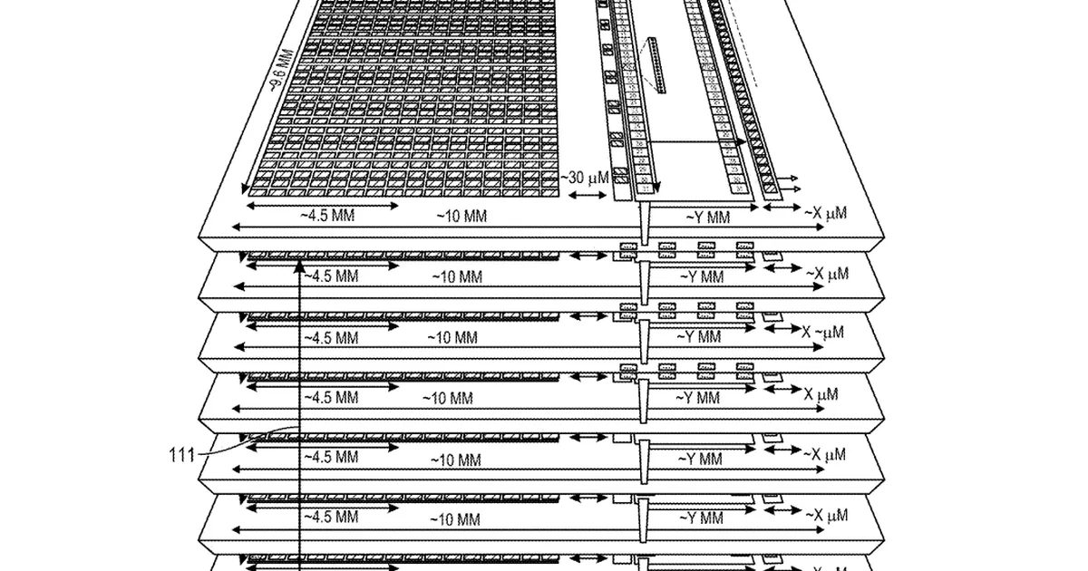
Intel 申请 XBM 内存架构专利以降低 AI 芯片成本

本文如何被排名

Signal score
0 / 100
Composite score across the factors below. Higher = stronger signal that this story matters right now.
Newsworthiness bucket
Research
一项关于新型内存架构的专利申请。
Source corroboration
5 independent sources
Strong cross-source corroboration — multiple independent publishers covered this within the clustering window.
Topics
infra, product
Editorial topic classification. Feeds into how the story surfaces on /topic/<slug> hub pages and into the per-entity coverage mix.
AI-industry relevance
High
Clearly on-topic for AI-industry coverage.
Story freshness
93 days old
Aged out of breaking-news scoring windows; ranking reflects the durable signal from the full source set.
Coverage growth since scoring
+1 source(s) since last score
New sources have picked up this story since our last re-score. Score will update on the next scoring pass.

完整方法见我们的编辑标准。

报道来源 [5]

  1. 36氪 (36Kr) TIER_1 中文(ZH) ·

    Intel专利揭示新型XBM内存架构,旨在绕过HBM硅中介层以降低AI内存成本

    7月8日消息,英特尔一项近日公开的专利申请显示,公司正研发名为XBM(Cross-Batch Memory)的新型高带宽内存架构,旨在通过取消HBM所需的硅中介层、采用UCIe互连及内置冗余修复机制,降低先进封装成本并缓解AI芯片“内存墙”瓶颈。专利显示,XBM采用后端晶体管(BEOL)DRAM堆叠设计,可在保持与HBM4相近封装尺寸的同时提升可扩展性,并支持缺陷修复以提高良率。(界面)

  2. Tom's Hardware TIER_1 English(EN) · Etiido Uko ·

    研究人员将HBM侧放以应对AI内存的散热瓶颈 — 韩国V-Die和日本MOSAIC设计有望实现更高带宽、更密集堆叠和更凉爽的未来GPU

    Researchers in Korea and Japan have proposed sideways-stacked DRAM designs that could push future AI memory beyond conventional HBM limits by improving cooling, bandwidth, and capacity while reducing reliance on TSV-heavy vertical stacks.

  3. Tom's Hardware TIER_1 English(EN) · Etiido Uko ·

    Intel专利揭示新型XBM内存架构,摒弃HBM昂贵的硅中介层——后端晶体管DRAM堆栈采用UCIe连接和内置修复,以缓解AI的内存瓶颈

    Intel’s XBM patent proposes an HBM alternative that uses backend-transistor DRAM, UCIe chiplet links, and repair logic to reduce packaging costs and complexity.

  4. Mastodon — fosstodon.org TIER_1 English(EN) · [email protected] ·

    研究人员将HBM侧放以应对AI内存散热瓶颈 — 韩国V-Die和日本MOSAIC设计… 韩国和日本的研究人员提出了侧放方案

    Researchers turn HBM on its side to tackle AI memory’s heat wall — Korean V-Die and Japanese MOSAIC desig… Researchers in Korea and Japan have proposed sideways-stacked DRAM designs that could push future AI memory beyond conventional HBM limits by improving cooling, bandwidth, a…

  5. Mastodon — fosstodon.org TIER_1 English(EN) · [email protected] ·

    Intel专利揭示新型XBM内存架构,摒弃HBM昂贵的硅中介层——后端晶体管DRAM堆栈采用UCIe连接和内置修复

    Intel patent reveals new XBM memory architecture that ditches HBM's costly silicon interposer — backend-transistor DRAM stack uses UCIe links and built-in repair to … Intel’s XBM patent proposes an HBM alternative that uses backend-transistor DRAM, UCIe chiplet links, and repair …