PulseAugur
实时 07:34:15
中文(ZH) IBM发布全球首款亚纳米芯片技术

IBM发布首个采用堆叠晶体管的亚纳米级芯片技术

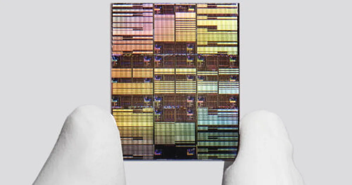
IBM宣布了其新型“亚纳米”(0.7纳米或7埃)芯片工艺的重大进展。这项突破采用了新颖的“纳米堆叠”架构,通过垂直堆叠晶体管来实现近乎翻倍的密度。该公司声称,这项创新可以带来性能提升高达50%或能效提高70%的芯片,从而解决AI数据中心面临的关键功耗挑战。IBM预计这项技术可以将芯片扩展再延长十年,并可能在五年内实现量产。 AI

影响 这项进展可能显著提高数据中心AI的性能和能效,并可能将芯片扩展再延长十年。

排序理由 IBM宣布了一项具有特定节点名称和架构的新芯片技术。[lever_c_demoted from frontier_release: ic=10 ai=0.7]

在 36氪 (36Kr) 阅读 →

AI 生成摘要 · Google Gemini · 来自 10 个来源。 我们如何撰写摘要 →

IBM发布首个采用堆叠晶体管的亚纳米级芯片技术

报道来源 [10]

  1. 36氪 (36Kr) TIER_1 中文(ZH) ·

    IBM Releases World's First Nanosheet Chip Technology

    6月25日,IBM宣布在半导体技术领域取得重大突破,推出了全球首款“亚纳米”(sub-1nm)芯片工艺技术。该技术采用了革命性的“三维垂直堆叠”(NanoStack)晶体管架构,直接跨越至0.7纳米(即7埃米,Angstrom)节点。通过这种新型3D架构,IBM成功在指甲盖大小的芯片上集成了近1000亿个晶体管,晶体管密度较其2021年推出的2纳米芯片整整翻了一番。(界面)

  2. Engadget TIER_1 English(EN) · [email protected] (Igor Bonifacic) ·

    IBM says it has created the world's first sub-1 nanometer chip

    IBM says it has created the world's first sub-1 nanometer chip

  3. Forbes — Innovation TIER_1 English(EN) · John Koetsier, Senior Contributor ·

    IBM Unveils World’s First Sub-1nm Chip With 100 Billion 3D-Stacked Transistors

    IBM just unveiled the world's first sub 1-nanometer chip: 100 billion transistors. IBM also says they've produced functioning devices with this technology.

  4. Data Center Knowledge TIER_1 English(EN) · Shane Snider ·

    IBM Pushes AI Chip Design Forward with Sub-1 nm NanoStack

    IBM’s NanoStack transistor platform promises to extend chip scaling beyond nanosheets, offering improvements in AI performance, memory density, and energy efficiency.

  5. Ars Technica — AI TIER_1 English(EN) · Jeremy Hsu ·

    IBM claims world’s first sub-1 nanometer chip technology

    IBM’s nanostack transistors could boost chip performance or energy efficiency.

  6. Mastodon — sigmoid.social TIER_1 English(EN) · [email protected] ·

    IBM has unveiled what it calls the world's first sub-1 nanometer chip technology for AI data centres. The nanostack architecture packs nearly 100 billion transi

    IBM has unveiled what it calls the world's first sub-1 nanometer chip technology for AI data centres. The nanostack architecture packs nearly 100 billion transistors onto a chip the size of a human fingernail - nearly double the transistor density of the previous generation. The …

  7. The Register — AI TIER_1 English(EN) ·

    IBM stacks up a sub-nanometer chip future

    Big Blue shows off process node it claims can scale down to 1 Angstrom

  8. Mastodon — fosstodon.org TIER_1 Italiano(IT) · [email protected] ·

    🚨 NEWS: IBM unveils sub-1 nanometer chip with nanostack architecture for AI data centers Key points in brief: 💡 IBM has announced a new architecture

    🚨 NEWS: IBM svela chip sub-1 nanometro con architettura nanostack per data center AI Ecco i punti chiave in breve: 💡 IBM ha annunciato una nuova architettura di chip che integra quasi 100 miliardi di transistor su una superficie grande quanto un'unghia, raddoppiando la densità ri…

  9. Mastodon — mastodon.social TIER_1 English(EN) · sagalinked ·

    📰 IBM has unveiled chip technology with 100 billion transistors, twice the density of its previous state-of-the-art, potentially extending Moore's Law another d

    📰 IBM has unveiled chip technology with 100 billion transistors, twice the density of its previous state-of-the-art, potentially extending Moore's Law another decade and paving the way for faster and more energy-efficient computers. 🔗 https://www. technologyreview.com/2026/06/2 5…

  10. r/singularity TIER_2 English(EN) · /u/truecakesnake ·

    IBM Debuts World’s First Sub-1 Nanometer Chip Technology

    &#32; submitted by &#32; <a href="https://www.reddit.com/user/truecakesnake"> /u/truecakesnake </a> <br /> <span><a href="https://newsroom.ibm.com/2026-06-25-ibm-debuts-worlds-first-sub-1-nanometer-chip-technology">[link]</a></span> &#32; <span><a href="https://www.reddit.com/r/s…