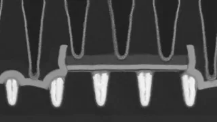
行业领导者imec、ASML和台积电已成功在300毫米晶圆上制造出50纳米间距的互补型二维材料晶体管,这是迈向后硅时代的重要一步。这项在IEEE/JSAP超大规模集成电路技术与电路研讨会上展示的突破性技术,利用单次极紫外光(EUV)光刻曝光即可制造出短至28纳米的沟道。集成晶体管表现出高开关比和近乎完美的开关特性,其中n沟道器件使用二硫化钼,p沟道器件使用二硒化钨或二硫化钨。通过颠倒传统晶体管制造工艺,将金属触点置于二维沟道下方,这项成就克服了以往的尺寸瓶颈。 AI
影响 这项晶体管技术的进步可能为未来更强大、更高效的人工智能硬件奠定基础。
排序理由 该集群报道了半导体制造领域的一项重大技术进步,涉及主要行业参与者以及晶体管尺寸缩放方面的突破。[lever_c_demoted from significant: ic=1 ai=0.7]
- 2D transistor
- ASML Holding
- extreme ultraviolet lithography
- Gouri Sankar Kar
- IEEE/JSAP Symposium on VLSI Technology and Circuits
- Intel
- molybdenum disulfide
- TSMC
- tungsten diselenide
- tungsten disulfide
AI 生成摘要 · Google Gemini · 来自 1 个来源。 我们如何撰写摘要 →