PulseAugur
实时 17:02:22
English(EN) Huawei unveils new scaling law and tech that narrows gap with TSMC, Samsung

华为发布突破制裁的芯片设计,声称到2031年实现1.4纳米级密度

华为宣布了一项名为“LogicFolding”的新芯片架构,旨在绕过美国制裁,并于2031年实现“1.4纳米级”晶体管密度。这项新设计基于优先考虑信号速度而非组件尺寸的“Tau Scaling Law”,允许堆叠逻辑电路将晶体管密度提高55%。该技术预计将在即将推出的Kirin智能手机处理器中首次亮相,之后将应用于AI和数据中心芯片,可能为受限的外国硬件提供替代方案。 AI

影响 这一发展可能为中国提供国内AI和数据中心芯片的替代品,可能影响全球供应链和竞争。

排序理由 该公告详细介绍了一家主要科技公司的新芯片架构和扩展定律,旨在规避国际制裁并与全球现有参与者竞争。

在 SCMP — Tech 阅读 →

AI 生成摘要 · Google Gemini · 来自 6 个来源。 我们如何撰写摘要 →
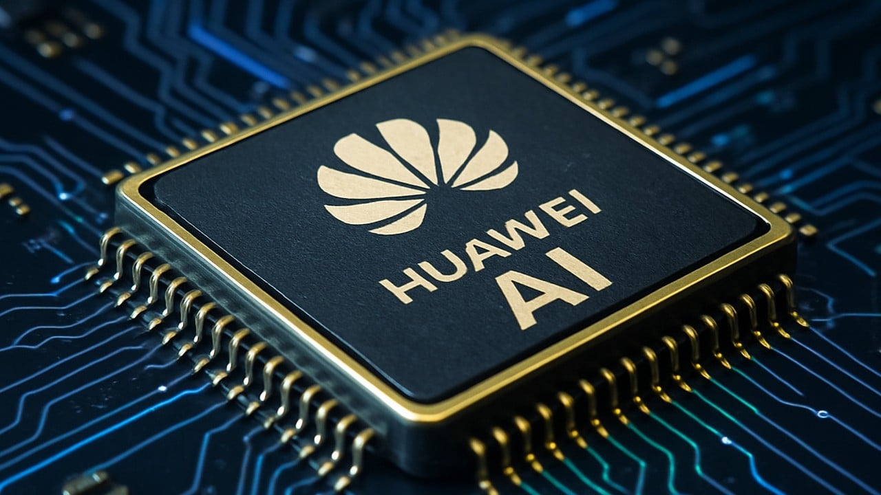
华为发布突破制裁的芯片设计,声称到2031年实现1.4纳米级密度

报道来源 [6]

  1. SCMP — Tech TIER_1 English(EN) · Howard Liu ·

    Meet He Tingbo: Huawei’s ‘chip queen’ trying to rewrite China’s semiconductor playbook

    When He Tingbo took the stage in Shanghai this week to unveil Huawei Technologies’ Tau (τ) Scaling Law, the message was about more than a new chip development framework. It was also a statement, showing how the most prominent Chinese technology company to have been subjected to U…

  2. SCMP — Tech TIER_1 English(EN) · Iris Deng,Ann Cao ·

    Another ‘DeepSeek moment’? Huawei milestone alters China trajectory in chip race: analysts

    Huawei Technologies’ unveiling of a chip architectural workaround to bypass US sanctions marks a major step towards China’s semiconductor self-sufficiency, giving Beijing powerful new leverage in its tech tug of war with Washington, analysts say. The Chinese tech giant captured g…

  3. SCMP — Tech TIER_1 English(EN) · Coco Feng,Ann Cao,Iris Deng ·

    Huawei’s new chip scaling law aims to sidestep ASML chokepoint but hurdles remain: analysts

    Huawei Technologies has engineered a workaround to one of China’s most crippling chipmaking bottlenecks, but analysts warn that the nation’s path to semiconductor independence is still constrained by manufacturing challenges. The US-sanctioned tech giant on Monday introduced a ne…

  4. SCMP — Tech TIER_1 English(EN) · Ann Cao,Iris Deng ·

    华为发布新技术,缩小与台积电、三星的差距

    Huawei Technologies has unveiled a new scaling law and chip architecture intended to deliver transistor performance equivalent to a 1.4-nanometre process node – representing the leading edge of semiconductor development – in a few years without relying on advances in lithography …

  5. Tom's Hardware TIER_1 English(EN) · Etiido Uko ·

    华为声称通过1.4nm级芯片实现“制裁规避”突破,晶体管密度提高55%——该公司声称新的LogicFolding芯片架构可绕过EUV限制,并推出“Tau Scaling Law”取代摩尔定律

    Huawei Technologies unveiled a new “LogicFolding” chip design framework built on its proprietary Tau scaling law, claiming it can dramatically boost transistor density and power efficiency without EUV lithography — potentially helping China narrow the gap with TSMC and Nvidia des…

  6. Mastodon — fosstodon.org TIER_1 English(EN) · [email protected] ·

    华为声称通过2031年前的1.4纳米级芯片实现突破,打破制裁,晶体管密度提高55%…华为技术公司发布了新的“LogicFolding”芯片

    Huawei claims sanctions-busting breakthrough with 1.4nm-class chips by 2031, claims 55% higher transistor… Huawei Technologies unveiled a new “LogicFolding” chip design framework built on its proprietary Tau scaling law, claiming it can dramatically boost transistor density and p…