PulseAugur
实时 09:59:19
English(EN) Leading-edge foundry roadmaps for TSMC, Intel and Samsung — outlining the path to 1.4nm nodes and beyond

TSMC、Intel、Samsung在1.4纳米芯片生产路线图上出现分歧

TSMC、Intel和Samsung都在生产使用2纳米级别工艺技术的芯片,其中Samsung和TSMC已于2025年中后期开始量产。它们的未来路线图存在显著差异:TSMC优先考虑可预测的扩展和专业化,Samsung专注于通过迭代节点变体来提高良率,而Intel则采取激进策略,采用环绕栅极晶体管和背面供电等先进技术,目标是在2027-2028年实现1.4纳米节点。 AI

影响 先进的芯片制造进展直接影响AI硬件的性能和可用性,从而影响未来的AI开发和部署。

排序理由 文章详细介绍了主要晶圆代工厂的先进半导体制造路线图,包括其在1.4纳米节点方面的进展,这对科技行业具有重要意义。

在 Tom's Hardware 阅读 →

AI 生成摘要 · Google Gemini · 来自 2 个来源。 我们如何撰写摘要 →
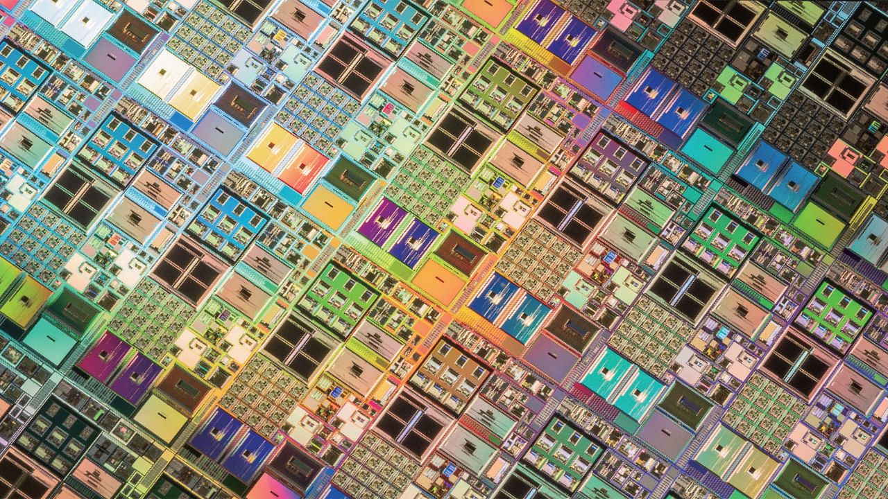
TSMC、Intel、Samsung在1.4纳米芯片生产路线图上出现分歧

报道来源 [2]

  1. Tom's Hardware TIER_1 English(EN) · Anton Shilov ·

    台积电、英特尔和三星的领先工艺路线图——迈向1.4纳米及更高节点

    All three leading foundries have now entered the 2nm era, but their paths from now on diverge sharply: TSMC bets on predictability, Intel wagers on aggressive architectural shifts, and Samsung's primary focus is on improving yields.

  2. Mastodon — mastodon.social TIER_1 English(EN) · [email protected] ·

    台积电、英特尔和三星的领先工艺路线图——描绘通往1.4纳米及更高节点的道路 三家领先的代工厂现已进入2纳米时代

    Leading-edge foundry roadmaps for TSMC, Intel and Samsung — outlining the path to 1.4nm nodes and beyond All three leading foundries have now entered the 2nm era, but their paths from now on diverge sharply: TSMC bets on predictability, Intel wagers on aggressive architectural sh…