PulseAugur
中
实时 17:26:14
English(EN) Nano imprint lithography aims to attack the main weakness of e-beam lithography which is low throughput. The required device pattern is written onto a mold usin

纳米压印光刻为光子芯片制造提供高吞吐量替代方案

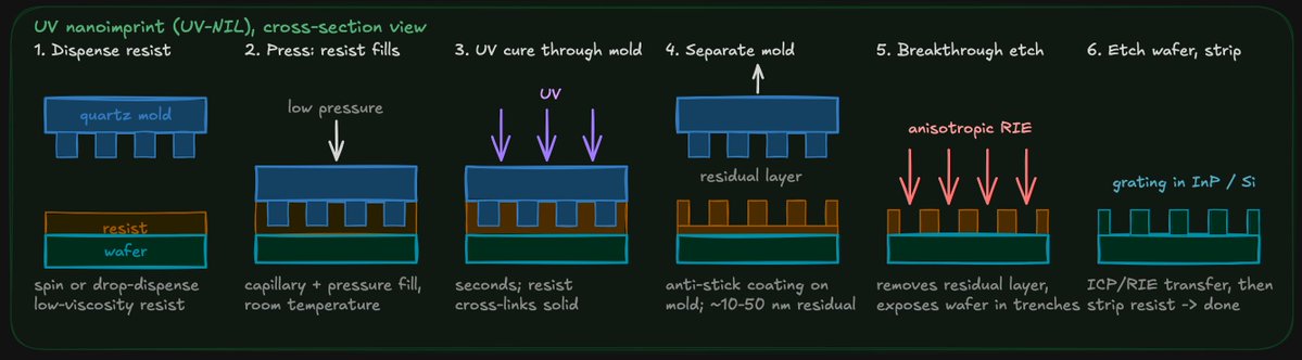
纳米压印光刻(NIL)正被探索作为电子束光刻制造光子集成电路(PICs)的一种高吞吐量替代方案。虽然电子束光刻提供精度和灵活性,但其低吞吐量使其不适用于大规模生产。EVG在台湾半导体展上展示的NIL技术使用模具将图案压印到晶圆上,有可能以高得多的速度实现相似的分辨率。然而,挑战仍然存在,包括表面清洁度、精确套准、模具退化和晶圆平整度。 AI

排序理由 该集群讨论了一种光子芯片的制造技术,详细介绍了其与现有方法的潜在优势和挑战。[lever_c_demoted from research: ic=3 ai=0.4]

在 X — SemiAnalysis 阅读 →

AI 生成摘要 · Google Gemini · 来自 3 个来源。 我们如何撰写摘要 →
纳米压印光刻为光子芯片制造提供高吞吐量替代方案

本文如何被排名

Signal score
0 / 100
Composite score across the factors below. Higher = stronger signal that this story matters right now.
Newsworthiness bucket
Tool
该集群讨论了一种光子芯片的制造技术,详细介绍了其与现有方法的潜在优势和挑战。[lever_c_demoted from research: ic=3 ai=0.4]
Source corroboration
3 independent sources
Multiple independent publishers reporting the same story raises confidence that it's real and newsworthy.
Topics
infra, product
Editorial topic classification. Feeds into how the story surfaces on /topic/<slug> hub pages and into the per-entity coverage mix.
AI-industry relevance
Standard
On-topic for AI-industry coverage; kept in the public index.
Story freshness
6 days old
Aged out of breaking-news scoring windows; ranking reflects the durable signal from the full source set.

完整方法见我们的编辑标准。

报道来源 [3]

  1. X — SemiAnalysis TIER_1 English(EN) · SemiAnalysis_ ·

    纳米压印光刻旨在克服电子束光刻低通量这一主要弱点。所需的器件图案被刻在模具上,使用

    Nano imprint lithography aims to attack the main weakness of e-beam lithography which is low throughput. The required device pattern is written onto a mold using e-beam lithography. Then this mold is used to stamp the feature onto many wafers. This theoretically ensures a similar…

  2. X — SemiAnalysis TIER_1 English(EN) · SemiAnalysis_ ·

    目前,大多数光子芯片制造采用电子束光刻。在此过程中,电子束手动扫描晶圆以蚀刻单个芯片

    Currently, most photonic chip fabrication uses e-beam lithography. In this process, an electron beam manually scans the wafer to inscribe the individual chip features. Electron beam lithography allows high precision and allows for the flexibility to inscribe arbitrary patterns, h…

  3. X — SemiAnalysis TIER_1 English(EN) · SemiAnalysis_ ·

    在台湾半导体展上,EVG介绍了在光子集成电路大规模制造和激光制造中使用纳米压印光刻(NIL)的技术

    In Semicon Taiwan, EVG had described the use of Nano-Imprint Lithography (NIL) in the mass manufacture of Photonic Integrated Circuits and for laser manufacturing. NIL is especially useful to define periodic structures within a photonic chip such as grating couplers or microlens