PulseAugur
实时 21:09:58
English(EN) TSMC’s moat is bigger than PPA, EUV, or yield. It is the EDA/IP ecosystem wrapped around the fab. (1/8)🧵 https://t.co/800d2FClQC

台积电的竞争护城河建立在EDA/IP生态系统之上,而非仅仅是工艺技术

SemiAnalysis认为,台积电的竞争优势不在于工艺技术(PPA、EUV、良率),而在于其庞大的电子设计自动化(EDA)和知识产权(IP)生态系统。这个多年来不断壮大的生态系统包括了众多预先认证的接口模块和IP供应商。这个全面的网络降低了设计风险,并增加了三星和英特尔等竞争对手吸引台积电客户的成本,从而有效地形成了强大的平台锁定。 AI

影响 强调了生态系统锁定,而非仅仅是原始性能,如何塑造半导体制造业的竞争格局。

排序理由 来自SemiAnalysis关于半导体行业竞争护城河的分析。

在 X — SemiAnalysis 阅读 →

AI 生成摘要 · Google Gemini · 来自 8 个来源。 我们如何撰写摘要 →
台积电的竞争护城河建立在EDA/IP生态系统之上,而非仅仅是工艺技术

报道来源 [8]

  1. X — SemiAnalysis TIER_1 English(EN) · SemiAnalysis_ ·

    We discussed this and more in our EDA Market Primer recently. (8/8)https://t.co/FQWwEcZCq6

    We discussed this and more in our EDA Market Primer recently. (8/8)https://t.co/FQWwEcZCq6

  2. X — SemiAnalysis TIER_1 English(EN) · SemiAnalysis_ ·

    Samsung and Intel are not only chasing TSMC’s process roadmap. They are chasing the TSMC-EDA/IP feedback loop. (7/8)

    Samsung and Intel are not only chasing TSMC’s process roadmap. They are chasing the TSMC-EDA/IP feedback loop. (7/8)

  3. X — SemiAnalysis TIER_1 English(EN) · SemiAnalysis_ ·

    And it works both ways. Foundries use EDA/IP ecosystems to deepen platform lock-in. EDA companies use foundry qualification to get a front-row seat with designe

    And it works both ways. Foundries use EDA/IP ecosystems to deepen platform lock-in. EDA companies use foundry qualification to get a front-row seat with designers, then pull through tools, verification, and implementation software later in the design cycle. (6/8)

  4. X — SemiAnalysis TIER_1 English(EN) · SemiAnalysis_ ·

    Customers do not switch foundries just because a competitor claims better PPA. They switch only if the whole design risk stack moves with them. That is the foun

    Customers do not switch foundries just because a competitor claims better PPA. They switch only if the whole design risk stack moves with them. That is the foundry moat. (5/8)

  5. X — SemiAnalysis TIER_1 English(EN) · SemiAnalysis_ ·

    Every additional pre-qualified SerDes, HBM, PCIe, UCIe, memory, and chiplet interface block lowers tape-out risk at TSMC and raises the cost of moving a flagshi

    Every additional pre-qualified SerDes, HBM, PCIe, UCIe, memory, and chiplet interface block lowers tape-out risk at TSMC and raises the cost of moving a flagship ASIC to Samsung Foundry or Intel Foundry. (4/8)

  6. X — SemiAnalysis TIER_1 English(EN) · SemiAnalysis_ ·

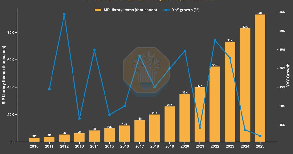
    TSMC’s certified Silicon IP library grew from 3K items in 2010 to 93K in 2025. 31x growth. (3/8)

    TSMC’s certified Silicon IP library grew from 3K items in 2010 to 93K in 2025. 31x growth. (3/8)

  7. X — SemiAnalysis TIER_1 English(EN) · SemiAnalysis_ ·

    TSMC’s Open Innovation Platform has turned Synopsys, Cadence, Arm, Rambus, Alphawave, and dozens of IP vendors into a pre-validated tape-out network. And that m

    TSMC’s Open Innovation Platform has turned Synopsys, Cadence, Arm, Rambus, Alphawave, and dozens of IP vendors into a pre-validated tape-out network. And that moat is measurable. (2/8)

  8. X — SemiAnalysis TIER_1 English(EN) · SemiAnalysis_ ·

    TSMC’s moat is bigger than PPA, EUV, or yield. It is the EDA/IP ecosystem wrapped around the fab. (1/8)🧵 https://t.co/800d2FClQC

    TSMC’s moat is bigger than PPA, EUV, or yield. It is the EDA/IP ecosystem wrapped around the fab. (1/8)🧵 https://t.co/800d2FClQC