PulseAugur
实时 12:22:24
English(EN) IBM goes sub-1nm, develops 0.7nm-class technology — offering up to 50% higher performance and 70% higher energy efficiency compared to IBM's 2nm-class node IBM'

IBM 发布采用纳米堆叠晶体管的亚纳米级芯片技术

IBM 宣布在半导体制造领域取得突破,开发出 0.7 纳米级别制造技术,这是业界首个亚纳米级工艺。这项新技术采用了纳米堆叠晶体管,将互补的 n 型和 p 型晶体管垂直堆叠在两个晶圆上,而不是并排放在单个晶圆上。这种创新的方法可以独立优化每种类型的晶体管,与 IBM 先前的 2 纳米级别节点相比,在性能和能效方面取得了显著的改进。 AI

影响 芯片制造的这项进步可能带来更强大、更节能的硬件,从而加速 AI 的开发和部署。

排序理由 IBM 宣布了一项代表半导体制造重大进步的新制造技术。

在 Mastodon — mastodon.social 阅读 →

AI 生成摘要 · Google Gemini · 来自 2 个来源。 我们如何撰写摘要 →
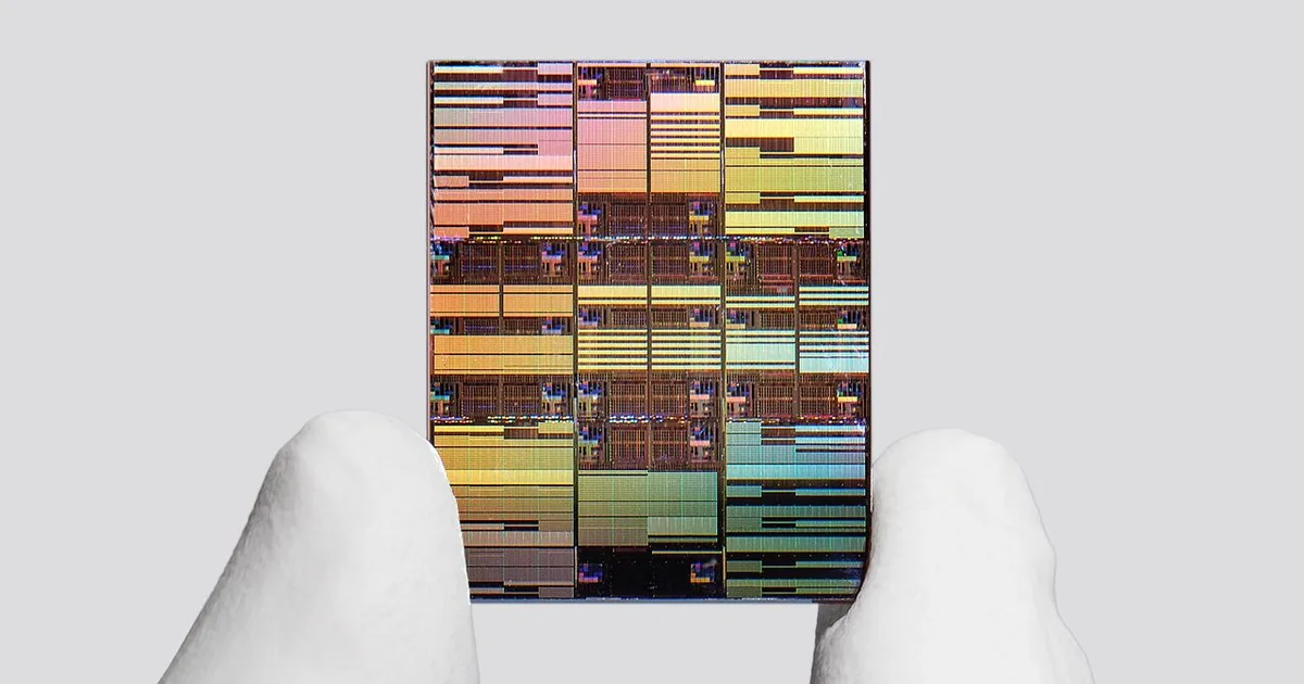
IBM 发布采用纳米堆叠晶体管的亚纳米级芯片技术

报道来源 [2]

  1. Tom's Hardware TIER_1 English(EN) · Anton Shilov ·

    IBM 率先实现 0.7nm 级技术,性能提升高达 50%,能效比提升 70%

    IBM's new 0.7nm-class fabrication process uses nanostack transistors, requires 2x more FEOL steps for massive improvements in performance, power, and area.

  2. Mastodon — mastodon.social TIER_1 English(EN) · [email protected] ·

    IBM 研发 0.7nm 级技术,性能提升高达 50%,能效提升高达 70%(相较于 IBM 的 2nm 级节点)

    IBM goes sub-1nm, develops 0.7nm-class technology — offering up to 50% higher performance and 70% higher energy efficiency compared to IBM's 2nm-class node IBM's new 0.7nm-class fabrication process uses nanostack transistors, requires 2x more FEOL steps for massive improvements i…