PulseAugur
实时 15:41:56
English(EN) While this design allows two cell arrays to share the same base periphery logic wafer and enables higher bit density per package, the additional yield loss from

NAND闪存制造商Kioxia和三星推出多阵列键合架构

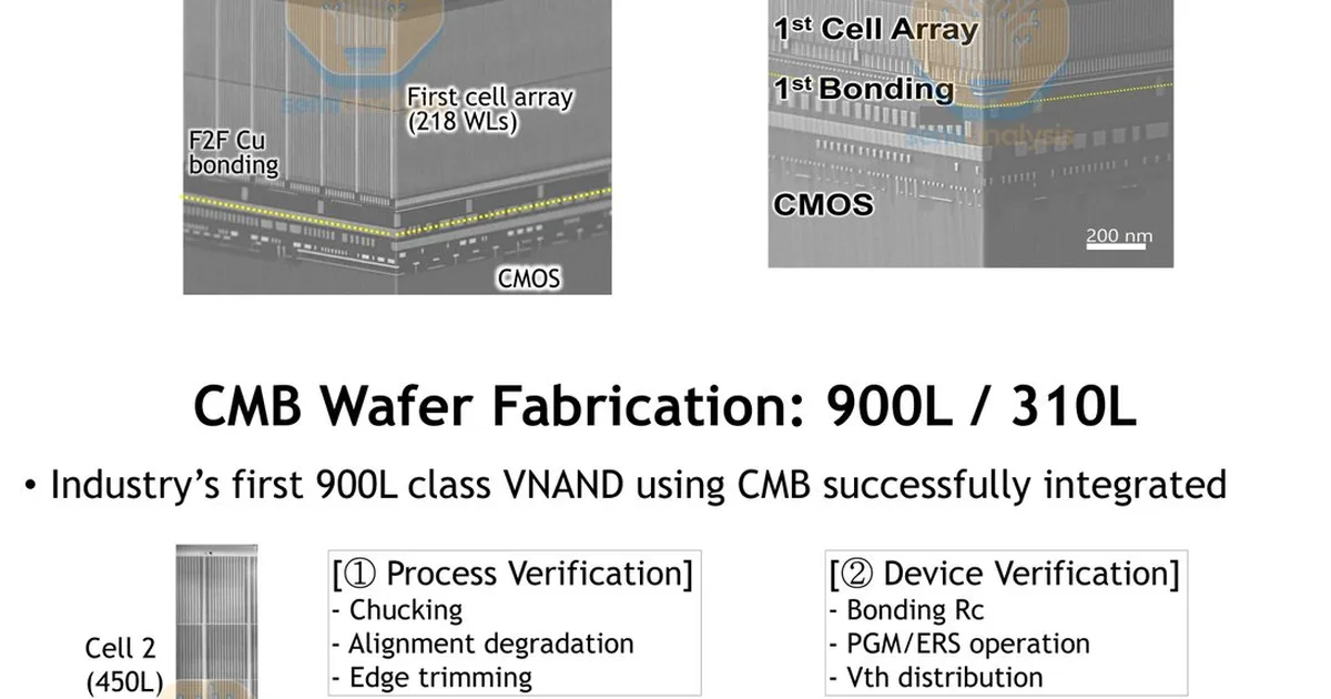
SemiAnalysis报道称,Kioxia和三星推出了多阵列混合键合NAND架构,旨在实现1000层以上以提高密度。Kioxia的样品包括一个双218L堆叠以管理机械集成问题和一个双17L堆叠用于电气测试。三星的Cell Multi-Bonding样品包括一个双450L机械样品和一个双155L电气样品。然而,分析表明,额外的混合键合步骤导致的良率损失增加以及单元阵列之间电气匹配的需要可能会抵消成本节省,尤其是在产能受限的环境中,因为在这种环境中,每个晶圆厂的比特输出较低是不受欢迎的。 AI

影响 数据存储密度增加的潜力可能会影响AI模型的训练和部署。

排序理由 该集群讨论了在半导体行业的研究和开发领域内,在会议上展示的新NAND闪存架构。

在 X — SemiAnalysis 阅读 →

AI 生成摘要 · Google Gemini · 来自 2 个来源。 我们如何撰写摘要 →
NAND闪存制造商Kioxia和三星推出多阵列键合架构

报道来源 [2]

  1. X — SemiAnalysis TIER_1 English(EN) · SemiAnalysis_ ·

    While this design allows two cell arrays to share the same base periphery logic wafer and enables higher bit density per package, the additional yield loss from

    While this design allows two cell arrays to share the same base periphery logic wafer and enables higher bit density per package, the additional yield loss from having another hybrid bonding step in the stack and requiring both upper and lower cell arrays to be electrically

  2. X — SemiAnalysis TIER_1 English(EN) · SemiAnalysis_ ·

    In our current capacity-limited environment, the last thing the industry needs is lower bit output per fab from lower stacking yield. Both Kioxia and Samsung un

    In our current capacity-limited environment, the last thing the industry needs is lower bit output per fab from lower stacking yield. Both Kioxia and Samsung unveiled multi-array hybrid bonded NAND architectures at VLSI 2026 as a path to 1000+ layers for maximum density. Kioxia's…