PulseAugur
实时 04:01:53
English(EN) IBM just broke through the nanometer wall with a 0.7 nm chip built on a novel 3D "nanostack" transistor design; the first sub-1 nm chip ever made. ⚛️ Nearly 100

IBM 发布全球首款 0.7 纳米芯片,为人工智能硬件进步铺平道路

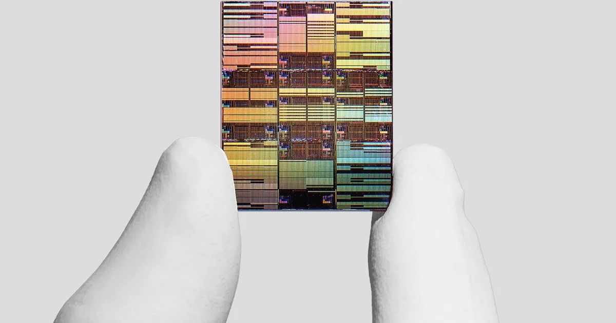
IBM 开发出了全球首款采用 0.7 纳米工艺的芯片,利用了新型 3D "nanostack" 晶体管设计。这项突破将近 1000 亿个晶体管集成在一起,与 2 纳米芯片相比,能效提高了高达 70%。该开发预计将实现半导体技术十年以上的进一步扩展,并对人工智能工作负载和开放计算基础设施具有重大意义。 AI

影响 这项在芯片密度和能效方面的突破可以显著加速人工智能工作负载和更强大的人工智能硬件的开发。

排序理由 重大行业举措:IBM 宣布新的半导体工艺技术。 [lever_c_demoted from significant: ic=1 ai=0.7]

在 Mastodon — mastodon.social 阅读 →

AI 生成摘要 · Google Gemini · 来自 1 个来源。 我们如何撰写摘要 →

IBM 发布全球首款 0.7 纳米芯片,为人工智能硬件进步铺平道路

报道来源 [1]

  1. Mastodon — mastodon.social TIER_1 English(EN) · tgio ·

    IBM 刚刚凭借基于新型 3D "nanostack" 晶体管设计的 0.7 纳米芯片突破了纳米尺度瓶颈;这是有史以来第一款亚纳米级芯片。⚛️ 接近 100

    IBM just broke through the nanometer wall with a 0.7 nm chip built on a novel 3D "nanostack" transistor design; the first sub-1 nm chip ever made. ⚛️ Nearly 100B transistors, up to 70% energy savings vs 2 nm chips, and a roadmap projected for 10+ more years of scaling. Big implic…