PulseAugur
EN
LIVE 13:08:14

Cerebras explores wafer-on-wafer bonding for AI chip memory boost

Cerebras is developing a wafer-on-wafer bonding technique to enhance its AI chips, addressing the scaling limitations of SRAM. This approach involves bonding a second wafer, potentially containing additional SRAM or compute capabilities, onto their existing Wafer Scale Engine (WSE). While facing significant thermo-mechanical and bonding challenges, this innovation aims to overcome the trade-offs between memory and compute on a single wafer. AI

IMPACT Cerebras's wafer-on-wafer bonding could overcome SRAM scaling limits, potentially enabling more powerful AI hardware.

RANK_REASON The cluster discusses a novel technical approach to chip design and manufacturing, which is a form of research and development.

Read on X — SemiAnalysis →

AI-generated summary · Google Gemini · from 4 sources. How we write summaries →
Cerebras explores wafer-on-wafer bonding for AI chip memory boost

How we ranked this

Signal score
0 / 100
Composite score across the factors below. Higher = stronger signal that this story matters right now.
Newsworthiness bucket
Research
The cluster discusses a novel technical approach to chip design and manufacturing, which is a form of research and development.
Source corroboration
4 independent sources
Strong cross-source corroboration — multiple independent publishers covered this within the clustering window.
Topics
infra, product
Editorial topic classification. Feeds into how the story surfaces on /topic/<slug> hub pages and into the per-entity coverage mix.
AI-industry relevance
High
Clearly on-topic for AI-industry coverage.
Story freshness
115 days old
Aged out of breaking-news scoring windows; ranking reflects the durable signal from the full source set.

Full methodology in our editorial standards.

COVERAGE [4]

  1. X — SemiAnalysis TIER_1 English(EN) · SemiAnalysis_ ·

    Cerebras has an escape: wafer-on-wafer bonding a second wafer to add SRAM or compute. They're seriously exploring it, already showing a DRAM wafer hybrid bonded

    Cerebras has an escape: wafer-on-wafer bonding a second wafer to add SRAM or compute. They're seriously exploring it, already showing a DRAM wafer hybrid bonded onto the WSE for more fast memory. There are real thermo-mechanical and bond-wave challenges to clear, but going beyond

  2. X — SemiAnalysis TIER_1 English(EN) · SemiAnalysis_ ·

    Here's the trap. When the chip is the whole wafer, you can't shrink your way to more SRAM and you can't make the wafer bigger. The only lever left is reallocati

    Here's the trap. When the chip is the whole wafer, you can't shrink your way to more SRAM and you can't make the wafer bigger. The only lever left is reallocating area, and more SRAM means less compute. A zero-sum tradeoff on silicon that's already maxed out. (3/4)

  3. X — SemiAnalysis TIER_1 English(EN) · SemiAnalysis_ ·

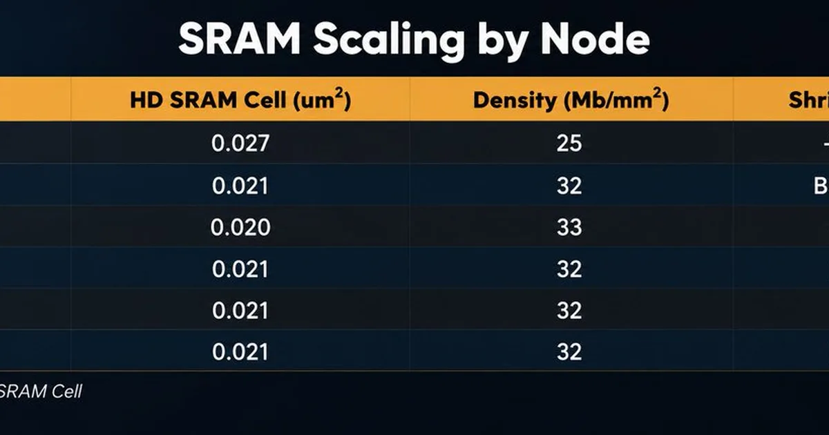
    Why the need for another wafer? SRAM has stopped scaling. That's a problem when SRAM is the whole pitch and 50% of the wafer. It's already on their roadmap: WSE

    Why the need for another wafer? SRAM has stopped scaling. That's a problem when SRAM is the whole pitch and 50% of the wafer. It's already on their roadmap: WSE-1 shipped 18GB of SRAM, WSE-2 jumped to 40GB, a healthy 2.2x. But WSE-3 advanced to just 44GB, a 10% gain across a full…

  4. X — SemiAnalysis TIER_1 English(EN) · SemiAnalysis_ ·

    Cerebras did what the industry calls impossible: turned an entire 46,225mm² wafer into one chip. Defects on silicon that big are inevitable, so they built in re

    Cerebras did what the industry calls impossible: turned an entire 46,225mm² wafer into one chip. Defects on silicon that big are inevitable, so they built in redundancy and custom per-batch masks that route around every bad core, landing near 100% usable wafers. The results: http…