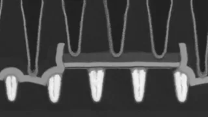
Industry leaders imec, ASML, and TSMC have successfully fabricated complementary 2D-material transistors at a 50nm pitch on a 300mm wafer, a significant step towards the post-silicon era. This breakthrough technology, presented at the IEEE/JSAP Symposium on VLSI Technology and Circuits, utilizes a single extreme ultraviolet (EUV) lithography exposure to create channels as short as 28nm. The integrated transistors demonstrated a high on/off current ratio and near-perfect switching behavior, with n-channel devices using molybdenum disulfide and p-channel devices using tungsten diselenide or disulfide. This achievement overcomes previous scaling bottlenecks by inverting the traditional transistor fabrication process, placing metal contacts beneath the 2D channel. AI
IMPACT This advancement in transistor technology could enable more powerful and efficient AI hardware in the future.
RANK_REASON This cluster reports on a significant technological advancement in semiconductor manufacturing, involving major industry players and a breakthrough in transistor scaling. [lever_c_demoted from significant: ic=1 ai=0.7]
- 2D transistor
- ASML Holding
- extreme ultraviolet lithography
- Gouri Sankar Kar
- IEEE/JSAP Symposium on VLSI Technology and Circuits
- Intel
- molybdenum disulfide
- TSMC
- tungsten diselenide
- tungsten disulfide
AI-generated summary · Google Gemini · from 1 sources. How we write summaries →