PulseAugur
EN
LIVE 03:57:06

Nano imprint lithography offers high-throughput alternative for photonic chip manufacturing

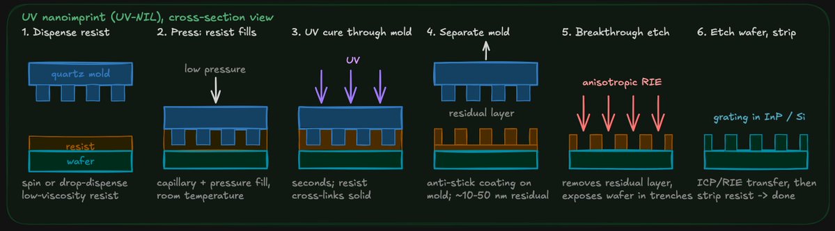
Nano imprint lithography (NIL) is being explored as a high-throughput alternative to electron beam lithography for manufacturing photonic integrated circuits (PICs). While e-beam lithography offers precision and flexibility, its low throughput makes it impractical for mass production. NIL, demonstrated by EVG at Semicon Taiwan, uses a mold to stamp patterns onto wafers, potentially achieving similar resolution at much higher speeds. However, challenges remain, including surface cleanliness, precise overlay, mold degradation, and wafer flatness. AI

RANK_REASON The cluster discusses a manufacturing technique for photonic chips, detailing its potential advantages and challenges compared to existing methods. [lever_c_demoted from research: ic=3 ai=0.4]

Read on X — SemiAnalysis →

AI-generated summary · Google Gemini · from 3 sources. How we write summaries →
Nano imprint lithography offers high-throughput alternative for photonic chip manufacturing

COVERAGE [3]

  1. X — SemiAnalysis TIER_1 English(EN) · SemiAnalysis_ ·

    Nano imprint lithography aims to attack the main weakness of e-beam lithography which is low throughput. The required device pattern is written onto a mold usin

    Nano imprint lithography aims to attack the main weakness of e-beam lithography which is low throughput. The required device pattern is written onto a mold using e-beam lithography. Then this mold is used to stamp the feature onto many wafers. This theoretically ensures a similar…

  2. X — SemiAnalysis TIER_1 English(EN) · SemiAnalysis_ ·

    Currently, most photonic chip fabrication uses e-beam lithography. In this process, an electron beam manually scans the wafer to inscribe the individual chip fe

    Currently, most photonic chip fabrication uses e-beam lithography. In this process, an electron beam manually scans the wafer to inscribe the individual chip features. Electron beam lithography allows high precision and allows for the flexibility to inscribe arbitrary patterns, h…

  3. X — SemiAnalysis TIER_1 English(EN) · SemiAnalysis_ ·

    In Semicon Taiwan, EVG had described the use of Nano-Imprint Lithography (NIL) in the mass manufacture of Photonic Integrated Circuits and for laser manufacturi

    In Semicon Taiwan, EVG had described the use of Nano-Imprint Lithography (NIL) in the mass manufacture of Photonic Integrated Circuits and for laser manufacturing. NIL is especially useful to define periodic structures within a photonic chip such as grating couplers or microlens