PulseAugur
EN
LIVE 20:57:45

TSMC's competitive moat built on EDA/IP ecosystem, not just process tech

SemiAnalysis argues that TSMC's competitive advantage lies not in process technology (PPA, EUV, yield) but in its extensive Electronic Design Automation (EDA) and intellectual property (IP) ecosystem. This ecosystem, which has grown significantly over the years, includes numerous pre-qualified interface blocks and IP vendors. This comprehensive network reduces design risk and increases the cost for competitors like Samsung and Intel to lure away TSMC's customers, effectively creating a strong platform lock-in. AI

IMPACT Highlights how ecosystem lock-in, rather than just raw performance, shapes competition in semiconductor manufacturing.

RANK_REASON Analysis from SemiAnalysis discussing competitive moats in the semiconductor industry.

Read on X — SemiAnalysis →

AI-generated summary · Google Gemini · from 8 sources. How we write summaries →
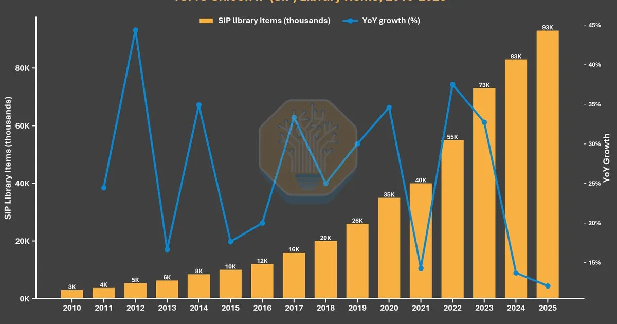
TSMC's competitive moat built on EDA/IP ecosystem, not just process tech

COVERAGE [8]

  1. X — SemiAnalysis TIER_1 English(EN) · SemiAnalysis_ ·

    We discussed this and more in our EDA Market Primer recently. (8/8)https://t.co/FQWwEcZCq6

    We discussed this and more in our EDA Market Primer recently. (8/8)https://t.co/FQWwEcZCq6

  2. X — SemiAnalysis TIER_1 English(EN) · SemiAnalysis_ ·

    Samsung and Intel are not only chasing TSMC’s process roadmap. They are chasing the TSMC-EDA/IP feedback loop. (7/8)

    Samsung and Intel are not only chasing TSMC’s process roadmap. They are chasing the TSMC-EDA/IP feedback loop. (7/8)

  3. X — SemiAnalysis TIER_1 English(EN) · SemiAnalysis_ ·

    And it works both ways. Foundries use EDA/IP ecosystems to deepen platform lock-in. EDA companies use foundry qualification to get a front-row seat with designe

    And it works both ways. Foundries use EDA/IP ecosystems to deepen platform lock-in. EDA companies use foundry qualification to get a front-row seat with designers, then pull through tools, verification, and implementation software later in the design cycle. (6/8)

  4. X — SemiAnalysis TIER_1 English(EN) · SemiAnalysis_ ·

    Customers do not switch foundries just because a competitor claims better PPA. They switch only if the whole design risk stack moves with them. That is the foun

    Customers do not switch foundries just because a competitor claims better PPA. They switch only if the whole design risk stack moves with them. That is the foundry moat. (5/8)

  5. X — SemiAnalysis TIER_1 English(EN) · SemiAnalysis_ ·

    Every additional pre-qualified SerDes, HBM, PCIe, UCIe, memory, and chiplet interface block lowers tape-out risk at TSMC and raises the cost of moving a flagshi

    Every additional pre-qualified SerDes, HBM, PCIe, UCIe, memory, and chiplet interface block lowers tape-out risk at TSMC and raises the cost of moving a flagship ASIC to Samsung Foundry or Intel Foundry. (4/8)

  6. X — SemiAnalysis TIER_1 English(EN) · SemiAnalysis_ ·

    TSMC’s certified Silicon IP library grew from 3K items in 2010 to 93K in 2025. 31x growth. (3/8)

    TSMC’s certified Silicon IP library grew from 3K items in 2010 to 93K in 2025. 31x growth. (3/8)

  7. X — SemiAnalysis TIER_1 English(EN) · SemiAnalysis_ ·

    TSMC’s Open Innovation Platform has turned Synopsys, Cadence, Arm, Rambus, Alphawave, and dozens of IP vendors into a pre-validated tape-out network. And that m

    TSMC’s Open Innovation Platform has turned Synopsys, Cadence, Arm, Rambus, Alphawave, and dozens of IP vendors into a pre-validated tape-out network. And that moat is measurable. (2/8)

  8. X — SemiAnalysis TIER_1 English(EN) · SemiAnalysis_ ·

    TSMC’s moat is bigger than PPA, EUV, or yield. It is the EDA/IP ecosystem wrapped around the fab. (1/8)🧵 https://t.co/800d2FClQC

    TSMC’s moat is bigger than PPA, EUV, or yield. It is the EDA/IP ecosystem wrapped around the fab. (1/8)🧵 https://t.co/800d2FClQC