PulseAugur
EN
LIVE 15:26:18

NAND flash makers Kioxia and Samsung unveil multi-array bonding architectures

SemiAnalysis reports that Kioxia and Samsung have introduced multi-array hybrid bonded NAND architectures aimed at achieving over 1000 layers for increased density. Kioxia's samples include a dual-218L stack to manage mechanical integration issues and a dual-17L stack for electrical testing. Samsung's Cell Multi-Bonding samples feature a dual-450L mechanical sample and a dual-155L electrical sample. However, the analysis suggests that the increased yield loss from additional hybrid bonding steps and the need for electrical matching between cell arrays may offset cost savings, particularly in a capacity-constrained environment where lower bit output per fab is undesirable. AI

IMPACT Potential for increased data storage density could impact AI model training and deployment.

RANK_REASON The cluster discusses new NAND flash architectures presented at a conference, which falls under research and development in the semiconductor industry.

Read on X — SemiAnalysis →

AI-generated summary · Google Gemini · from 2 sources. How we write summaries →
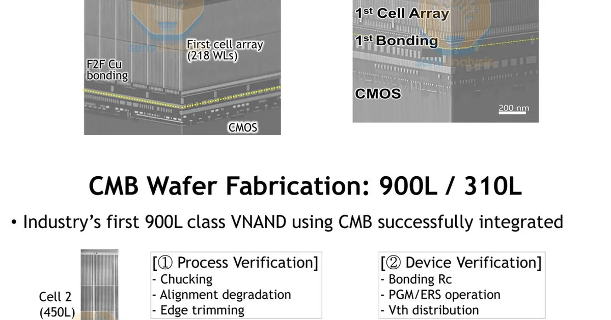
NAND flash makers Kioxia and Samsung unveil multi-array bonding architectures

COVERAGE [2]

  1. X — SemiAnalysis TIER_1 English(EN) · SemiAnalysis_ ·

    While this design allows two cell arrays to share the same base periphery logic wafer and enables higher bit density per package, the additional yield loss from

    While this design allows two cell arrays to share the same base periphery logic wafer and enables higher bit density per package, the additional yield loss from having another hybrid bonding step in the stack and requiring both upper and lower cell arrays to be electrically

  2. X — SemiAnalysis TIER_1 English(EN) · SemiAnalysis_ ·

    In our current capacity-limited environment, the last thing the industry needs is lower bit output per fab from lower stacking yield. Both Kioxia and Samsung un

    In our current capacity-limited environment, the last thing the industry needs is lower bit output per fab from lower stacking yield. Both Kioxia and Samsung unveiled multi-array hybrid bonded NAND architectures at VLSI 2026 as a path to 1000+ layers for maximum density. Kioxia's…