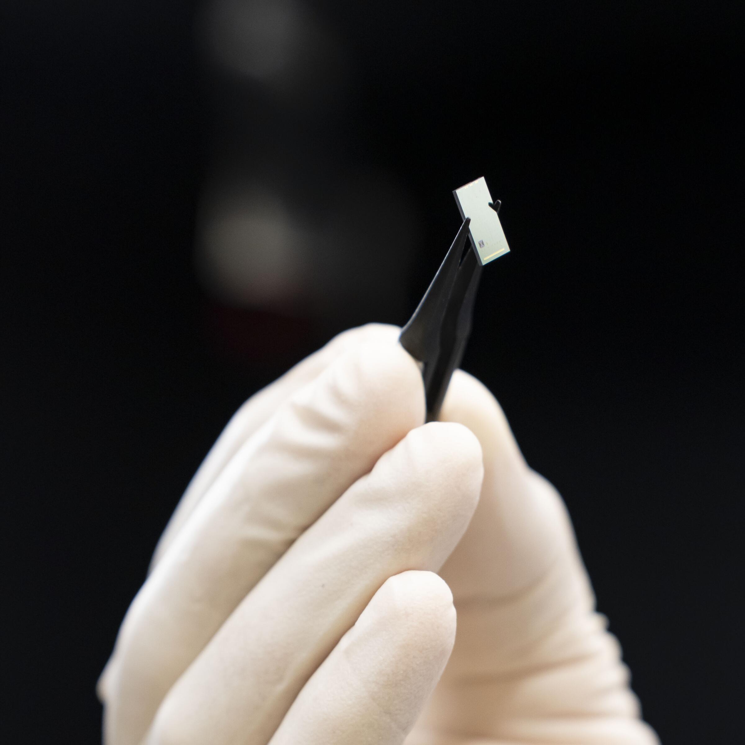
NIST researchers have developed a novel packaging technique for photonic integrated circuits, enabling them to function in extreme environments such as deep space, nuclear reactors, and high-temperature industrial settings. This advancement utilizes a hydroxide catalysis bonding (HCB) method, which creates a durable, inorganic bond between optical fibers and the chips, overcoming the limitations of traditional adhesives. The breakthrough promises to expand the application of high-speed, low-power photonic technologies into previously inaccessible demanding conditions, with potential for future large-scale manufacturing. AI
Summary written by gemini-2.5-flash-lite from 1 source. How we write summaries →
RANK_REASON The development of a new packaging technique for photonic chips by NIST researchers represents a significant research advancement in materials science and engineering for specialized applications.