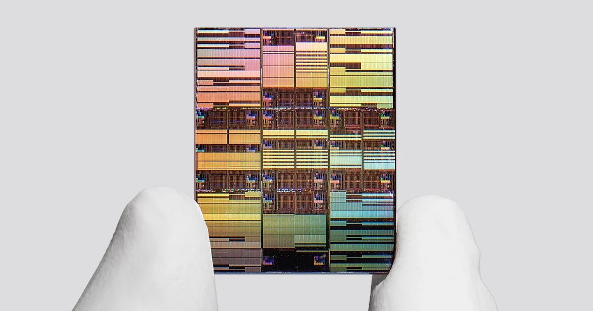
IBM has developed a groundbreaking 0.7nm-class fabrication technology, marking the industry's first sub-1nm manufacturing process. This new technology utilizes nanostack transistors, stacking complementary n-type and p-type transistors vertically across two wafers instead of the traditional side-by-side placement on a single wafer. This innovative approach promises significant improvements, offering up to 50% higher performance and 70% greater energy efficiency compared to IBM's previous 2nm-class node. AI
IMPACT This advancement in chip manufacturing could lead to more powerful and energy-efficient hardware, potentially accelerating AI development and deployment.
RANK_REASON Significant advancement in semiconductor manufacturing technology by a major industry player. [lever_c_demoted from significant: ic=1 ai=0.7]
- 0.7nm-class technology
- 2021
- 2nm-class node
- 7 angstroms
- China Foreign Exchange Trade System
- CMOS
- IBM
- nanosheet gate-all-around transistors
- nanostack transistors
AI-generated summary · Google Gemini · from 1 sources. How we write summaries →